03 // The Diamond Substrate
WHY CARBON-12 DIAMOND IS THE OPTIMAL TIER 1 HOST
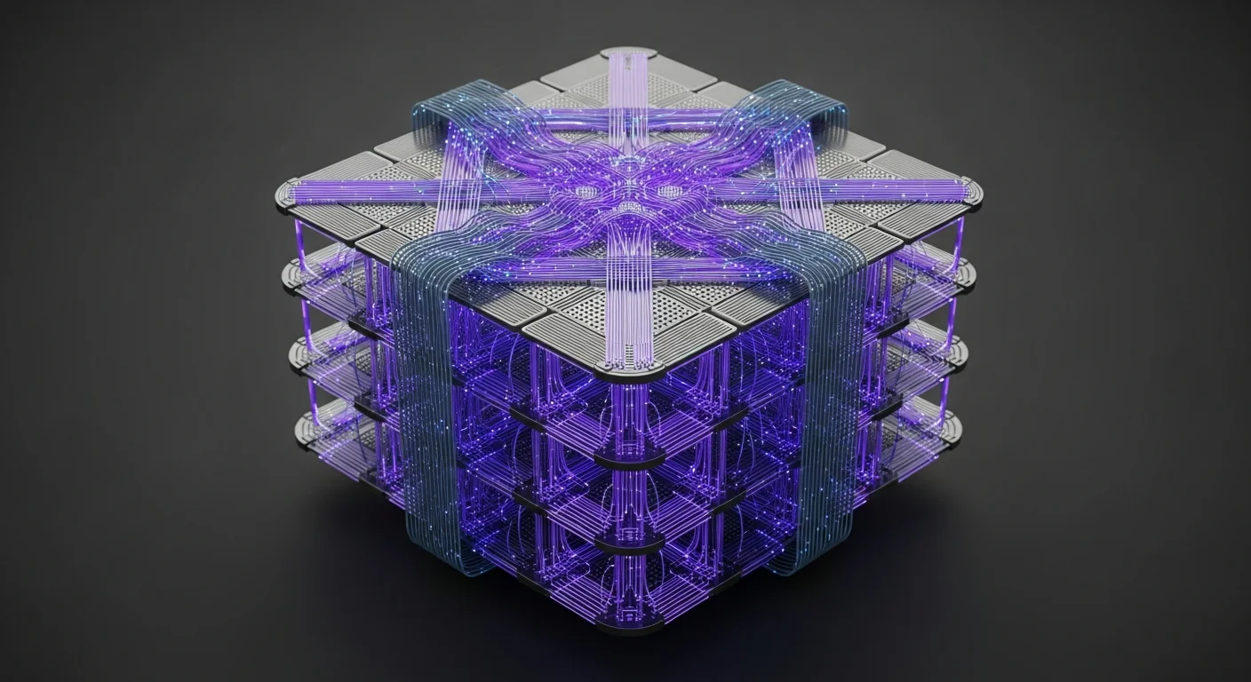
FIG 1.0: NITROGEN-VACANCY DIAMOND — 3D GATE LATTICE
Every photonic processor requires a substrate — a material through which light propagates, interacts, and computes. Silicon photonics uses doped silicon-on-insulator wafers borrowed from the electronics industry. Silicon works for this purpose, but it is a compromise: silicon has an indirect bandgap that makes it a poor light emitter, mediocre thermal conductivity, and a refractive index that limits waveguide density.
Diamond is the optimal Tier 1 substrate. Its properties are not incrementally better than silicon — they are categorically different in every metric relevant to single-particle control.
Thermal conductivity: 2,200 W/m·K — five times copper. Heat generated at I/O boundaries is conducted away from the active region without thermal management infrastructure. Optical transparency: continuous from deep ultraviolet through far infrared, covering the full photonic band required for Tier 1 and Tier 2 operations. Debye temperature: 2,230 K — phonon-mediated decoherence is suppressed at any temperature a human laboratory operates in. NV-center hosting: nitrogen-vacancy point defects trap single electrons whose spin states can be initialized, manipulated, and read out with light at room temperature. No cryogenics. No vacuum chamber.[6]
Aetheric Sciences uses isotopically pure Carbon-12 diamond grown by chemical vapor deposition (CVD). Carbon-13, which constitutes 1.1% of natural carbon, has a nuclear spin that couples to the NV electron spin and accelerates decoherence. Eliminating C-13 extends coherence times from microseconds to milliseconds — sufficient for thousands of gate operations per coherence window. The diamond is grown at Metallic Sciences using their Crystal Foundry CVD process, then transferred to Aetheric for NV implantation and waveguide etching.[11]
The Bekenstein bound defines the theoretical maximum information density for any region of space with finite energy. Diamond approaches the practical limit for a fabricated substrate: every NV center is a qubit, every lattice site is a potential gate, and the three-dimensional crystal structure provides cubic scaling where planar silicon provides only quadratic. The information density of a diamond photonic die exceeds any fabricated silicon node by orders of magnitude, not because the features are smaller, but because the features are volumetric.[12]