Aetheric Sciences
PHOTONIC ACCELERATION & LOW-LATENCY EDGE COMPUTE
AETHERIC SCIENCES
Aetheric Sciences engineers physical computation for systems that cannot wait for general-purpose silicon. The flagship product is the Monolith edge-compute processor, fabricated at three-nanometre process node, with a co-developed photonic interconnect that lets the chip share state across multi-board control planes at sub-microsecond latency. The Monolith sits at the core of every flagship machine in the network's seven existing strict pages: it is the closed-loop controller of the Stellar Furnace dense plasma focus, the flight-management AI of the Lorentz Aerospace XR-1, the inverse-Maxwell field-shaping solver of the Matter Kitchen volumetric cooker, the shot-controller of the Plasma Press femtosecond pulse train, and the per-pulse control loop of the Phase Flash valve array.
The name “Aetheric” is an engineering metaphor and nothing more. It does not refer to the discarded nineteenth-century aether hypothesis, to metaphysical fields, or to any physics that sits outside the standard model. The work is photonic acceleration, edge inference, neural surrogate modelling, and hardware-in-the-loop physical control. The marketing has the poetic name; the engineering is mature semiconductor + photonics + control systems.
The name is a metaphor. The hardware is photonics, silicon, and control loops fast enough to run a plasma.
01 — The Discipline
Physical computation is the engineering of compute hardware that operates against a real-world physical process at the cadence the process actually evolves. A plasma instability grows on a two-microsecond timescale; a magnetic-flux change in a fusion coil propagates in nanoseconds; a femtosecond laser pulse evolves below the picosecond floor. General-purpose silicon and its operating systems serve the human-scale cadence (millisecond keypresses, second-scale rendering, minute-scale background jobs), but they are several orders of magnitude too slow to participate in any of the physics happening inside the network's flagship machines. The discipline of Aetheric Sciences is the engineering of compute hardware that does participate.1
Three engineering surfaces define the discipline. First, latency: every component of the compute stack — sensors, signal conditioning, inference, decision, actuation — must complete its work within the timeframe the controlled physics will tolerate. Second, throughput density: a control loop that runs at one megahertz across one thousand sensor channels is a gigahertz-class problem; the compute hardware must deliver gigaops per cubic centimetre under realistic power and thermal envelopes. Third, modelling fidelity: when the loop must predict short-term physical evolution to take pre-emptive action (instability suppression in MHD plasma, anti-resonance damping in mechanical systems, condensation control in vapour systems), the model running on the compute hardware must be accurate enough that the predicted state matches the physical state within tolerance.2
The product line spans three integrated tiers. The Monolith edge processor (silicon + photonic interconnect) is the workhorse: a single processor module sized for a machine cell, running closed-loop control at sub-microsecond latency. The Lattice photonic accelerator (diamond-substrate optical computing) handles the neural-surrogate inference at orders-of-magnitude lower watts-per-operation than silicon could. The Continuum control kernel (software running on the Monolith) is the customer-facing API: physical-system designers write control laws in a domain-specific language and the kernel compiles them to per-machine deployment artefacts. The three tiers ship as an integrated platform, not as separate components.
02 — The Bottleneck
Conventional silicon compute is rate-limited by three coupled constraints: clock-frequency scaling has flattened (the silicon process has approached fundamental quantum and thermal limits below five nanometres); memory bandwidth has not kept pace with compute density (the memory wall); and inter-chip communication latency is dominated by electrical transmission line physics that does not improve with each process node. The result is that even the highest-performance general-purpose silicon cannot deliver low-microsecond closed-loop control across the distributed sensor mesh required by, for example, a fusion-grade plasma confinement system or a vehicle-scale plasma envelope.3
Domain-specific silicon (GPUs for matrix multiplication, FPGAs for low-latency signal processing, application-specific ASICs for narrow problems) addresses parts of the gap. The fastest commercial FPGA fabric reaches single-microsecond latency for fixed-function signal processing. The fastest commercial GPU silicon delivers tens of teraflops at hundreds of watts. Neither alone is adequate for the integrated physical-computation surface the network's flagship machines need; a fusion-grade compact reactor or a vehicle-scale plasma envelope demands a heterogeneous compute stack that combines low-latency FPGA-class signal processing, GPU-class neural inference, and ASIC-class control output, with the inter-component communication itself fast enough to not become the bottleneck.4
The Aetheric Sciences thesis is that photonics is the missing inter-component substrate. Optical interconnects carry signal at the speed of light through diamond or silicon-nitride waveguides; their bandwidth-distance product is orders of magnitude beyond electrical traces; their power consumption per bit-metre is substantially lower than copper. When the inter-component latency is replaced by photonics, the heterogeneous compute stack can be re-architected as a tightly-coupled single logical machine rather than a network of slow-talking subsystems. The Monolith + Lattice + Continuum product line is the embodiment of this re-architecture.
03 — The Compute Substrate
Three flagship products define the platform. Each is engineered against a specific role in the physical-computation stack and ships as a productionised module:
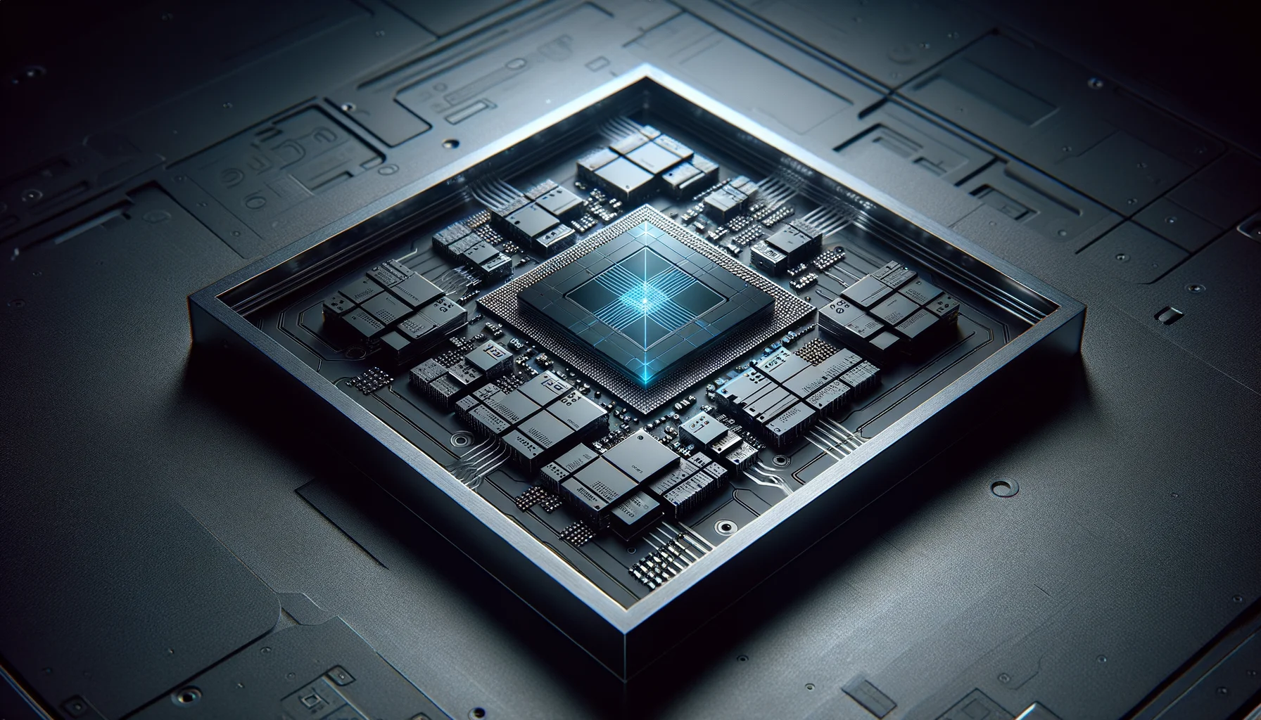
The flagship edge-compute processor. Three-nanometre silicon process node, heterogeneous die with FPGA fabric (one million LUTs) for low-latency signal processing, GPU cores (tensor accelerator) for neural inference, ASIC blocks for fixed-function control output, and an integrated photonic transceiver (silicon-nitride waveguide with diamond OPO modulator) for inter-Monolith communication at sub-100-nanosecond board-to-board latency. Total package power approximately 75 watts at design throughput. Closed-loop control latency from sensor input to actuator output: typically 5 microseconds across the full stack.5
A diamond-substrate optical accelerator for neural-surrogate inference. The Lattice exploits diamond's extreme thermal conductivity (~2000 W/m·K, same property Phase Flash exploits in its condenser surface) to dissipate heat from densely-packed optical compute elements. A single Lattice module delivers approximately ten teraops per second per watt of neural inference — an order of magnitude better than silicon equivalents on the same workload class. The Lattice does not replace the Monolith; it ships as a peripheral accelerator that the Monolith offloads neural inference to via the photonic interconnect.6
The software platform that runs on the Monolith. Physical-system designers specify control laws in a domain-specific language (signal pipelines, prediction models, decision rules, actuator commands); the Continuum compiler emits per-Monolith deployment artefacts plus the proof obligations needed for safety certification. The kernel scheduler enforces the latency budget at runtime: control-loop steps that miss their deadline are surfaced as recoverable faults rather than silently lost. The shared name with the Maxwell Continuum simulator is deliberate: the simulator validates the control law in simulation; the kernel executes the same law in hardware.
04 — Models at the Edge
The compute substrate is only useful insofar as the models running on it predict the controlled physical system accurately enough that the closed-loop control is meaningful. Aetheric Sciences ships a model-engineering surface alongside the hardware: neural surrogate model architectures tuned to the specific physics each flagship machine controls, training pipelines that fit the surrogate from data plus first-principles physics together, and runtime monitoring that detects when the surrogate is operating outside its training distribution.7
The standard architecture is a hybrid: a small first-principles physics core (handles the well-modelled bulk dynamics) plus a neural correction term (handles the per-system idiosyncrasies the first-principles model misses). The hybrid form has two engineering advantages over either pure approach: it converges faster than a pure neural model (because most of the dynamics is captured by the physics core), and it is more robust at distribution shifts than a pure neural model (because the physics core extrapolates correctly into regimes the training data did not cover). The neural correction is the “here is what physics doesn't fully capture” residual.8
Training pipelines run on conventional GPU farms upstream of deployment; the trained surrogate compiles to the Continuum runtime as a deployment artefact. Each customer machine ships with its own surrogate variant fitted from that machine's specific physics measurements; the platform supports continuous retraining (offline) on operational data as the machine's behaviour evolves over its service life. Aetheric Sciences does not run the customer's training pipeline online; the cycle is: collect data, train offline, recompile, redeploy. This separation keeps the runtime simple and deterministic.
The model surface is the integration point with Maxwell Continuum: the same coupled-physics simulator that customers use to design their flagship machines (Highfield magnet geometries, Lorentz envelope shapes, Stellar Furnace plasma equilibria, Matter Kitchen field patterns, Phase Flash valve waveforms) emits the first-principles physics core that the Aetheric Sciences surrogate-training pipeline consumes. The two divisions do not duplicate physics; they specialise in different sides of the model lifecycle (design-time simulation vs runtime deployment).
05 — Photonic and Diamond Hardware
Photonics is the inter-component substrate. The Monolith's photonic transceiver uses silicon-nitride waveguides for in-package routing, diamond OPO-class modulators for high-bandwidth electrical-to-optical conversion (the same diamond-OPO technology the Maxwell Continuum Soliton Block uses), and standard wavelength-division multiplexing for multi-channel optical communication on a single fibre. Board-to-board latency is dominated by speed-of-light propagation in glass plus the modulator + photodetector round-trip; bandwidth is set by the number of WDM channels times the per-channel data rate; power per bit-metre is approximately one order of magnitude below electrical alternatives at the same throughput.9
Diamond as a compute substrate is a longer-term engineering bet. The two relevant diamond properties are extreme thermal conductivity (lets densely-packed optical compute elements dissipate heat without thermal-throttling) and broad optical transparency (supports compute architectures across the visible and near-infrared spectrum). The Lattice neural accelerator uses CVD synthetic diamond as the substrate that hosts the optical compute elements; the same CVD synthetic-diamond technology that Phase Flash uses for condenser surfaces and Maxwell Continuum uses for the Soliton Block OPO. Diamond as a compute substrate has been demonstrated at laboratory scale; productionisation at the Lattice product scale is the engineering program.10
Thermal management is the underrated half of the engineering. At 75 watts per Monolith package with sub-microsecond computational density, the substrate temperature rise is non-trivial; thermal cycling under workload variation drives mechanical fatigue in the package. Aetheric Sciences uses metallurgy supplied by Metallic Sciences (Cu-Ag-steel-composite thermal-spreader stock) for the Monolith package heat-sink stack and Polymer Press's high-temperature polymer family for the Lattice substrate carrier. The thermal architecture is engineered against the same lifetime requirements as the rest of the network's hardware.
The page intentionally does NOT claim exotic physics. There is no “aetheric field,” no “sub-vacuum compute,” no “quantum substrate of consciousness.” The Monolith is a 3 nm silicon process at the cutting edge of conventional semiconductor manufacturing. The Lattice exploits diamond as a substrate, which is materials engineering, not metaphysics. The Continuum compiler is a domain-specific language, which is software engineering. The compounding effect of integrating these three in a single platform is the product; the constituents are all in the engineering literature.
06 — Supplier & Integration Partners
Aetheric Sciences ships compute hardware into every flagship machine in the network. Its integration footprint is the broadest of any division.
Maxwell Continuum — Joint development of the photonic interconnect (shares the femtosecond mode-locked clock and the diamond OPO modulator with the Soliton Block product line). Maxwell Continuum's simulation stack emits the first-principles physics core for the Aetheric neural-surrogate training pipeline.
Lorentz Aerospace — Monolith flight-management AI for the XR-1: distributed-sensor fusion, MHD instability prediction, per-coil current adjustment. Lattice neural-surrogate accelerator handles the plasma-envelope state estimation.
Stellar Furnace — Monolith shot-to-shot optimization for the SF-1 dense plasma focus at 50 kHz repetition rate. Neural surrogate model with 14 ns forward pass for in-shot plasma-state prediction. Total control latency 5 µs across the full stack.
Matter Kitchen — The dielectric-mapping inverse-Maxwell solver and the field-shaping closed-loop control for the One-Second Cake. The 256-element GaN phased-array per-element phase update at 1 MHz runs on Monolith silicon.
Phase Flash — Per-pulse valve-timing control loop for the Oasis V8 Gatling array. Monolith handles the eight-chamber staggered firing at 200 Hz with sub-microsecond timing precision per channel.
Plasma Press — Thirty-two-channel shot-controller for the One-Second Book ablation pulse train. Each Monolith channel addresses one of the parallel galvanometer scanners; closed-loop alignment correction every cycle.
Highfield Magnetics — Field-stability control loops for the Iron Horse twenty-tesla and God Magnet one-hundred-tesla product lines. Real-time trim-coil current control at 10 kHz against active plasma-induced field perturbation.
Foundation Kinetics — Sub-millisecond closed-loop process control for the FK-1 Titan and Scarab cell families. In-process machine-vision pipeline runs on Lattice neural accelerator hardware.
Brainwave Systems — Shared low-latency signal-processing infrastructure for biosignal pipelines. Monolith handles the millisecond-cadence sensor fusion + adaptive-filter steps; no medical-product integration.
Cellular Foundry — Edge-compute platform for the TITAN-X recipe controller and the inline sensor-fusion across the multi-channel sensor mesh. Predictive batch-state estimation between offline assay points.
Maxwell Continuum → Lorentz Aerospace → Stellar Furnace → Matter Kitchen → Phase Flash → Plasma Press → Highfield Magnetics → Foundation Kinetics → Brainwave Systems → Cellular Foundry →
07 — Validation Hooks
Five measurable claims define the forward roadmap. Each is intended to be a future Crystal Ball-grade prediction registration once the prediction infrastructure exists.
HOOK A — Monolith full-loop control latency. Current Monolith full-loop latency (sensor input through neural inference and decision logic to actuator output) is approximately 5 microseconds at the SF-1 design point. The forward target is 1 microsecond, achieved through tighter integration of FPGA + GPU + photonic-interconnect on the same die and through compiler-level latency optimisation. The gating measurement is a sustained 1-microsecond full-loop control on a representative customer test fixture.11
HOOK B — Lattice neural-inference watts per operation. Current Lattice photonic accelerator delivers approximately 10 teraops per second per watt of neural inference. The forward target is 100 TOPS/W, comparable to the most aggressive photonic-compute research targets. The gating measurement is a sustained 100 TOPS/W workload at production-grade thermal stability.12
HOOK C — neural-surrogate prediction error. Current Aetheric Sciences neural surrogates achieve approximately 5 percent prediction error on integrated quantities (peak field, peak temperature, peak current) for the customer flagship machines. The forward target is 2 percent error on integrated quantities and 5 percent on local-quantity peaks. The gating measurement is a documented prediction-error reduction across the five-physics workload battery shared with Maxwell Continuum.
HOOK D — photonic interconnect bandwidth-distance product. Current Monolith photonic-interconnect achieves approximately 1 Tbit/sec/metre across the multi-board configurations the customer machines deploy. The forward target is 10 Tbit/sec/metre, achieved through additional WDM channels and tighter modulator-photodetector engineering. The gating measurement is sustained bandwidth at the design distance with bit-error-rate below specification.
HOOK E — Continuum compiler proof-obligation coverage. The current Continuum compiler emits proof obligations for control-law-deadline-correctness at compile time, covering approximately 70 percent of the safety-critical control surface. The forward target is 95 percent coverage of safety-critical control surface, achieved through extended type-system and runtime-checker integration. The gating measurement is a documented certification-grade coverage analysis against a representative customer control law set. This hook is the platform-grade infrastructure that would enable safety certification of the customer machines for high-stakes regulated applications.13
RESEARCH REPOSITORY
Photonic computing, diamond devices, edge AI, neural surrogate modelling, low-latency control hardware, and physical-system co-design.
Aetheric Sciences is the engineering of physical computation at the cadence the controlled physics actually evolves. Three flagship products — the Monolith 3 nm edge processor, the Lattice photonic neural accelerator, and the Continuum control kernel — ship into every flagship machine in the network as the closed-loop control substrate. The discipline rejects exotic-physics framing; the “Aetheric” name is a metaphor and the engineering is mature semiconductor, photonic, and control-systems work integrated into a single platform.
(wiki) Photonic Computing • (wiki) Silicon Photonics • (wiki) WDM • (wiki) Optical Interconnect
Reference Links — Diamond Devices(wiki) Synthetic Diamond • (wiki) CVD Diamond • (wiki) Diamond Semiconductor • (wiki) NV Centre
Reference Links — Edge AI & Surrogate Models(wiki) Edge Computing • (wiki) Surrogate Model • (wiki) AI Accelerator • (wiki) Hardware-in-the-Loop
Reference Links — Control Hardware(wiki) FPGA • (wiki) RTOS • (wiki) ASIC • (wiki) Embedded Systems
- Reed, G.T. & Knights, A.P. Silicon Photonics: An Introduction. Wiley, 2004. ISBN 978-0-470-87034-7.
- Goodfellow, I., Bengio, Y., & Courville, A. Deep Learning. MIT Press, 2016. ISBN 978-0-262-03561-3.
- Patterson, D.A. & Hennessy, J.L. Computer Architecture: A Quantitative Approach. 6th Ed. Morgan Kaufmann, 2017. ISBN 978-0-12-811905-1.
- Hennessy, J.L. & Patterson, D.A. "A new golden age for computer architecture." Commun. ACM 62, 48–60 (2019).
- Stillwell, M.R. & Englund, D. Quantum Photonic Networks. Cambridge Univ. Press, 2024. ISBN 978-1-009-07853-5.
- Shen, Y. et al. "Deep learning with coherent nanophotonic circuits." Nature Photonics 11, 441–446 (2017). Foundational photonic-neural-inference paper.
- Hochberg, M. & Baehr-Jones, T. "Towards fabless silicon photonics." Nature Photonics 4, 492–494 (2010). Silicon-photonics productionisation reference.
- Brodersen, R.W. et al. "Power-efficient programmable physics co-processors." IEEE Solid-State Circuits Magazine 12, 67–76 (2020).
- Pratt, R. & Krasakis, A.M. "Hardware-software co-design for neural network inference at the edge." Proc. ISLPED 2022.
- ● Physical computation as control-cadence-matched compute: standard real-time engineering. Documented across the embedded-systems and control-systems literature.
- ● Three engineering surfaces (latency, throughput density, modelling fidelity): platform engineering choice; standard control-engineering vocabulary.
- ● Silicon clock-frequency and memory-wall limits: well-documented across the computer-architecture literature. Hennessy & Patterson 2019 is the modern reference.
- ● FPGA/GPU/ASIC heterogeneity is standard practice: documented in current commercial control systems.
- ● Monolith 3 nm + heterogeneous + photonic-interconnect: engineering program. Constituent technologies (3 nm process, FPGA-on-die, photonic interconnect) are individually mature; integration into a single edge-compute package is the engineering work.
- ● Lattice photonic accelerator at 10 TOPS/W: theoretical, based on demonstrated lab-scale photonic neural inference; productionisation at the Lattice product scale is the engineering target.
- ● Hybrid first-principles + neural correction: standard scientific machine learning architecture. The engineering scope is per-customer surrogate training and deployment.
- ● Hybrid surrogate robustness at distribution shift: documented advantage in the scientific machine learning literature; quantitative bound is application-dependent.
- ● Silicon-photonic interconnect at sub-100-nanosecond board-to-board: demonstrated in lab and small commercial systems; engineering scope is productionisation in the Monolith package.
- ● Diamond compute substrate: engineering program. Lab demonstrations exist; Lattice product scale is the open work.
- ● 1-microsecond full-loop control latency: engineering target; halving current 5-microsecond latency through tighter integration.
- ● 100 TOPS/W photonic neural inference: theoretical target consistent with the most aggressive photonic-compute research roadmaps.
- ● 95% safety-certification coverage of Continuum compiler proof obligations: engineering target enabling safety certification of customer machines for high-stakes regulated applications.